
 Hardware
A0 Base Board
ESP32-C6 carrier with power, USB-C, and two expansion slots (BUS1/BUS2).
A0 Base Board
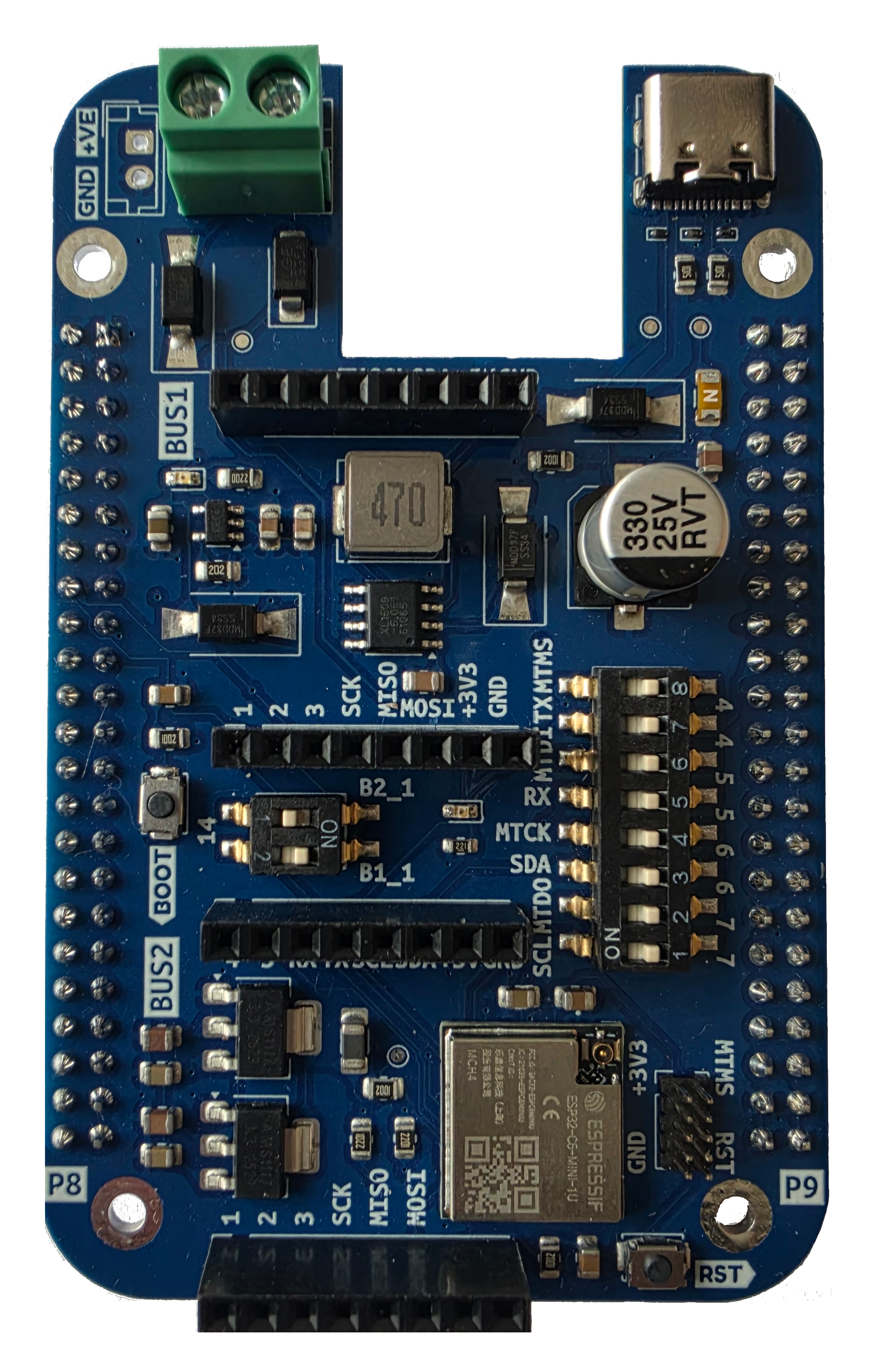
The A0 is the base board of the modular IoT gateway. It pushes all additional radio/cellular connectivity onto plug-in expansion modules.
Overview
A0 provides everything needed to power and run the gateway, while expansion slots (BUS1/BUS2) carry the connectivity:
- ESP32-C6 module on top — main compute plus Wi-Fi 6, Bluetooth 5 LE, and IEEE 802.15.4 connectivity. See the A0 Gateway overview for full specifications.
- Power:
- USB-C power input
- External power supply input (VIN terminal)
- Battery support via JST connector, with charging
- Expansion: two module slots, BUS1 and BUS2, where any of the following can be plugged in:
- SIM7080G — NB-IoT/LTE-M cellular + GNSS
- WMBUS — Wireless M-Bus metering radio
- E07-400M10S — Sub-GHz radio (400 MHz, 10 dBm)
- Any MikroE Click™ board, since the expansion slots use the Click footprint
Power
The board can be powered from USB-C, the external VIN terminal, or a single-cell Li-ion battery on the JST connector.
Power chain (see a0/power.kicad_sch):
- Battery path: MCP73831 single-cell Li-ion charge-management controller (U5) handles charging from the 5 V input to
VBAT. - 5 V rail: XL1509-5.0 buck converter (U6, 47 µH/2 A inductor L1) steps the input down to the board
FB_5V/+5Vrail. - 3.3 V rail: a pair of AMS1117-3.3 LDOs (U7/U8) regulate down to the
+3V3rail that feeds the ESP32-C6 module and the expansion slots.
Expansion Slots
BUS1 is the pair of 8-pin headers J1 + J3. BUS2 is the pair J4 + J2. Each slot carries SPI, UART, I2C, five mikroBUS-compatible control lines, and both power rails.
BUS1 Pinout (J1 + J3)
| Pin | Signal | ESP32-C6 | Notes |
|---|---|---|---|
| J1 pin 1 | MiBUS1_1 | via U1 switch | mikroBUS AN |
| J1 pin 2 | MiBUS1_2 | GPIO1 | mikroBUS RST — WMBUS SDN / SIM7080G PWRKEY |
| J1 pin 3 | MiBUS1_3 | GPIO2 | mikroBUS CS — SPI chip-select |
| J1 pin 4 | SCK | GPIO20 | SPI clock (shared BUS1/BUS2) |
| J1 pin 5 | MISO | GPIO19 | SPI MISO (shared BUS1/BUS2) |
| J1 pin 6 | MOSI | GPIO18 | SPI MOSI (shared BUS1/BUS2) |
| J1 pin 7 | +3V3 | — | Module power — use this, not J3 pin 7 |
| J1 pin 8 | GND | — | Ground |
| J3 pin 1 | MiBUS1_4 | GPIO3 | mikroBUS PWM — SIM7080G RING |
| J3 pin 2 | MiBUS1_5 | GPIO0 | mikroBUS INT — SIM7080G CTS (via JP3, see module page) |
| J3 pin 3 | MiBUS1_RX | GPIO16 | UART RX — SIM7080G TX |
| J3 pin 4 | MiBUS1_TX | GPIO17 | UART TX — SIM7080G RX |
| J3 pin 5 | SCL | — | I2C clock (shared BUS1/BUS2) |
| J3 pin 6 | SDA | — | I2C data (shared BUS1/BUS2) |
| J3 pin 7 | FB_5V | — | +5 V rail — never power 3.3 V modules from here |
| J3 pin 8 | GND | — | Ground |
BUS2 Pinout (J4 + J2)
BUS2 mirrors BUS1 with its own control and UART lines. SPI (SCK/MISO/MOSI) and I2C (SCL/SDA) are shared across both slots; only one module should drive them at a time.
| Pin | Signal | Notes |
|---|---|---|
| J4 pin 1 | MiBUS2_1 | mikroBUS AN |
| J4 pin 2 | MiBUS2_2 | mikroBUS RST |
| J4 pin 3 | MiBUS2_3 | mikroBUS CS — via U1 switch (shared with DTR path) |
| J4 pin 4 | SCK | SPI clock (shared) |
| J4 pin 5 | MISO | SPI MISO (shared) |
| J4 pin 6 | MOSI | SPI MOSI (shared) |
| J4 pin 7 | +3V3 | Module power |
| J4 pin 8 | GND | Ground |
| J2 pin 1 | MiBUS2_4 | mikroBUS PWM |
| J2 pin 2 | MiBUS2_5 | mikroBUS INT |
| J2 pin 3 | MiBUS2_RX | UART RX (via SW5 — mutually exclusive with JTAG) |
| J2 pin 4 | MiBUS2_TX | UART TX (via SW5 — mutually exclusive with JTAG) |
| J2 pin 5 | SCL | I2C clock (shared; see DCD note on the SIM7080G page) |
| J2 pin 6 | SDA | I2C data (shared; via SW5) |
| J2 pin 7 | +5V | +5 V rail — never power 3.3 V modules from here |
| J2 pin 8 | GND | Ground |
Use the 3V3 pin, not the 5V pin: on BUS1, J1 pin 7 supplies +3V3 while J3 pin 7 supplies +5V (
FB_5V). The same applies on BUS2 (J4 pin 7 = +3V3, J2 pin 7 = +5V). All in-house modules are 1.8–3.6 V parts — power them from the +3V3 pin only.
mikroBUS Mapping
The five MiBUSx_y control lines follow the mikroBUS convention:
| Base-board net | mikroBUS name | Function |
|---|---|---|
| MiBUS1_1 / MiBUS2_1 | AN | Analog |
| MiBUS1_2 / MiBUS2_2 | RST | Reset |
| MiBUS1_3 / MiBUS2_3 | CS | SPI chip-select |
| MiBUS1_4 / MiBUS2_4 | PWM | PWM output |
| MiBUS1_5 / MiBUS2_5 | INT | Interrupt input |
UART (RX/TX) and I2C (SCL/SDA) plus SPI (SCK/MISO/MOSI) complete the Click-compatible footprint, so off-the-shelf Click boards plug directly into either slot.
SW5 — JTAG / BUS2 Selector
SW5 (8-position DIP, SMXS-08K-TP) multiplexes GPIO4 through GPIO7 between the JTAG debug header (J10) and the BUS2 UART and I2C lines (see a0/esp32-c6.kicad_sch):
- One side of the switch carries GPIO4/GPIO5/GPIO6/GPIO7 from the ESP32-C6 module.
- The other side carries the JTAG signals (
MTMS,MTDI,MTCK,MTD0) and the BUS2 signals (MiBUS2_TX,MiBUS2_RX,SDA,SCL).
Set SW5 toward the JTAG side to debug via J10, or toward the BUS2 side to use UART/I2C on a BUS2 module. The two uses are mutually exclusive — BUS2 UART or I2C and JTAG cannot be used simultaneously (see Getting Started).
Image
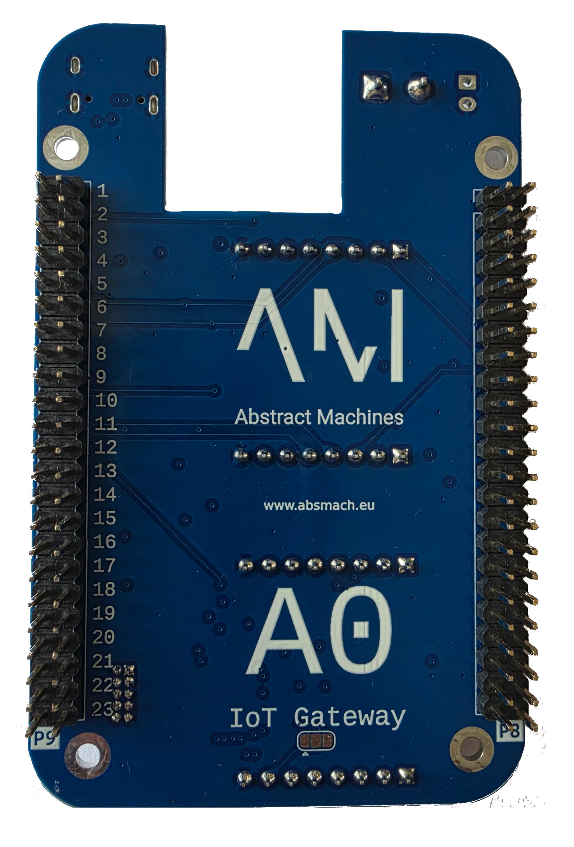
Front PCB
Back PCB
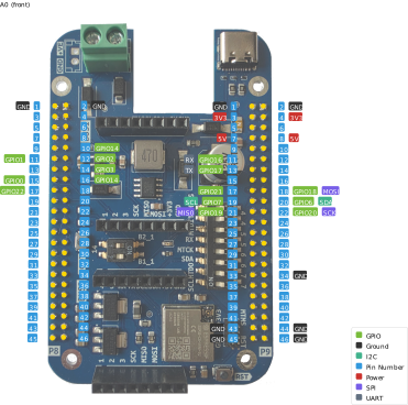
Front Pinout
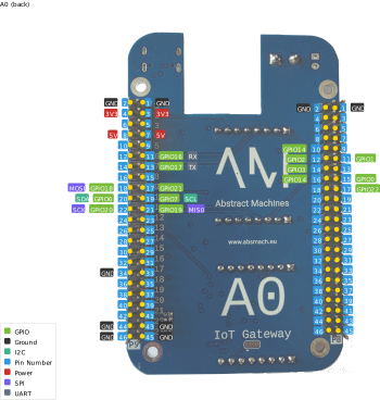
Back Pinout
Schematics & Sources
- Schematic (PDF) — GitHub
- KiCad sources — a0.kicad_sch · subsheets
esp32-c6,power,expansion,sim7080G,wmbus - Board README — GitHub
References
- ESP32-C6 — product page · datasheet (PDF)
- Bring-up — ESP32-C6 Boot Recovery